What Is Type 3 PCB?
Ever stumbled across the term “Type 3 PCB” and felt totally lost? You’re not alone. This phrase confuses engineers, buyers, and even seasoned designers. Why? Because it means three different things depending on who’s talking. In this guide, we’ll clear up every meaning. You’ll learn the standards, design rules, and where these boards actually shine. Let’s untangle it together.
Quick Answer: What Is a Type 3 PCB?
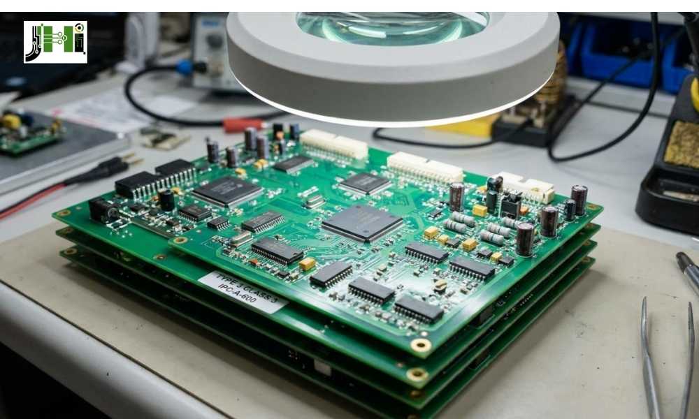
A Type 3 PCB is a multilayer printed circuit board built with plated through-holes. It typically has 4 to 8 layers of conductive copper. The term comes from the IPC-2222 standard, which classifies rigid PCBs by structure.
Here’s what makes it stand out:
- Multiple copper layers laminated together
- Plated through-holes connect every layer
- No blind or buried vias allowed
- Used in advanced electronics where simple boards can’t cope
It sounds simple. But it really isn’t.
Simple Definition of Type 3 PCB
A Type 3 PCB is a multilayer rigid board with plated through-holes that pass completely through every layer. Per IPC-2222, it sits one step above two-layer boards. It supports denser circuits without needing advanced via tech. Think of it as the workhorse of multilayer designs.
Why the Term “Type 3 PCB” Can Be Confusing
You see “Type 3 PCB” and assume it means one thing. Then you read another article saying something totally different. That’s because three groups use the term differently. IPC engineers mean structure. Quality buyers think of class. HDI specialists picture something else entirely. No wonder people get stuck. The good news? Once you see all three meanings, the fog lifts fast.
The Three Main Meanings of Type 3 PCB
People use “Type 3 PCB” in three different ways. Here’s the breakdown:
- IPC-2222 Type 3 – A multilayer board with plated through-holes only. No blind or buried vias. This is the most common meaning.
- IPC Class 3 – A reliability class, not a structure type. It means high-performance boards built for zero failure.
- HDI Type III – An advanced design under IPC-2226. It uses stacked microvias on both sides of the core.
Not the same thing. Same number, different worlds.
Type 3 PCB vs IPC Class 3 PCB
Here’s where most people slip up. “Type 3” and “Class 3” sound identical. They’re not. Type describes the physical build. Class describes the quality bar.
Quick comparison:
- Type 3 = Structure (multilayer with through-holes)
- Class 3 = Reliability level (high-performance, mission-critical)
- Type comes from IPC-2222
- Class comes from IPC-6011 and IPC-6012
- A board can be Type 3 AND Class 3 at the same time
Same number. Totally different meaning.
What Is an IPC Class 3 PCB?
An IPC Class 3 PCB is built for products where failure isn’t an option. Think pacemakers, jet engines, and missile guidance systems. These boards meet the strictest tolerances in the industry. Every dimension, plating layer, and inspection step gets held to tight limits.
You’ll see Class 3 boards in:
- Aerospace flight controls
- Life-support medical gear
- Military targeting systems
- Critical industrial safety loops
Is Type 3 PCB the Same as IPC Class 3 PCB?
No. They are not the same. Type tells you how the board is built. Class tells you how reliable it must be. Think of cars. “SUV” is the type. “Luxury grade” is the class. You can have a luxury SUV. But “SUV” alone doesn’t mean luxury. Same logic applies here.
Why IPC Class 3 PCBs Are Used in Critical Applications
Some failures cost money. Others cost lives. Class 3 boards exist for the second category. They go into systems where downtime isn’t a hiccup. It’s a disaster.
You’ll find them in:
- Heart monitors and ventilators
- Aircraft navigation units
- Defense communication gear
- Power grid control systems
If this fails, the cost is huge. That’s why every solder joint, plating layer, and trace gets checked twice.
IPC-2222 Type 3 PCB Explained
The IPC-2222 standard is the official rulebook for rigid PCB design. It groups boards into six types based on layer count and via structure. Type 3 sits in the middle. It’s a true multilayer board. But it sticks to plated through-holes only.
Key traits under IPC-2222:
- Three or more conductive layers
- Plated through-holes connect all layers
- No blind vias allowed
- No buried vias permitted
- Built using standard lamination methods
This makes Type 3 boards reliable, repeatable, and cost-friendly for medium-density designs.
Type 3 as a Multilayer PCB
A Type 3 board stacks multiple copper layers between insulation. Each layer holds part of the circuit. Picture a sandwich. Bread, cheese, meat, more bread. PCBs work the same way. Copper, prepreg, copper, prepreg. The more layers, the more routing space. That means smaller boards with bigger functionality.
Type 3 PCB Without Blind or Buried Vias
Here’s a key limit. Type 3 boards skip blind and buried vias. Every via must pass straight through the entire stack. Top to bottom. No exceptions. This keeps fabrication simpler and cheaper. But it also limits routing density. If you need tighter packing, you’ll move up to Type 4 or HDI designs.
Type 3 PCB vs Type 4 PCB
Both are multilayer boards. The big split is the via structure.
Type 3:
- Plated through-holes only
- Simpler to make
- Lower cost per board
Type 4:
- Adds blind and buried vias
- Higher routing density
- More complex fabrication
- Higher cost
Choose Type 3 for standard designs. Choose Type 4 when you need denser layouts.
HDI Type III PCB Explained
This is where things get advanced. HDI Type III comes from a different standard, IPC-2226. It’s not the same as IPC-2222 Type 3. Same number, different rulebook. HDI stands for High-Density Interconnect. These boards pack more circuits into less space using tiny microvias. Type III is the most complex level. It uses stacked microvias on both sides of the core. That allows ultra-dense routing for things like smartphones, smartwatches, and advanced medical implants. Think of HDI as the evolution of multilayer design.
What Is an HDI PCB?
An HDI PCB uses microvias to shrink board size while boosting performance. Microvias are tiny laser-drilled holes, often under 150 microns wide. These small holes allow trace routing in places where normal vias can’t fit.
You’ll see HDI boards in:
- Modern smartphones
- Wearable tech
- Compact medical devices
- High-speed networking gear
What Makes HDI Type III Different?
HDI Type III pushes density to the max.
Standout features:
- Stacked microvias on both sides of the core
- Two or more microvia layers per side
- Ultra-fine trace and space widths
- Sequential lamination process
- Highest interconnect density of any HDI type
It’s the choice when space is gold and performance can’t compromise.
HDI Type III PCB vs Conventional Type 3 PCB
Different worlds. Different costs.
Conventional Type 3 (IPC-2222):
- Plated through-holes only
- Standard layer count
- Lower cost
- Wider supplier base
HDI Type III (IPC-2226):
- Stacked microvias both sides
- Ultra-dense routing
- Much higher cost
- Fewer qualified makers
Pick conventional Type 3 for standard electronics. Pick HDI Type III when miniaturization matters most.
Key IPC Standards Related to Type 3 PCB
Quality PCBs follow rules. And the IPC standards are the gold-standard rulebook worldwide. These specs cover everything. From design and material picks to inspection and final testing. Following them isn’t optional for serious work.
Engineers group them into three buckets:
- Design standards – How to plan the board
- Performance standards – How it must perform
- Acceptance standards – How to inspect and test
Knowing which standard applies saves time, money, and warranty headaches.
IPC-6012 for Rigid PCB Performance
IPC-6012 sets performance rules for rigid PCBs. It defines what each class must achieve. Class 1, Class 2, and Class 3 all have different bars. Manufacturers use this to prove their boards meet the spec.
IPC-A-600 for Bare Board Acceptability
IPC-A-600 is the visual inspection bible for bare boards. It shows what passes. It shows what fails. Engineers use it to spot defects like voids, scratches, or plating problems before assembly.
IPC-A-610 for Assembly Acceptance
IPC-A-610 covers the assembled board. It defines solder joint quality, component placement, and finishing standards. This standard is the most widely used assembly quality reference in electronics.
IPC-2221 for General PCB Design
IPC-2221 is the foundation rulebook for all PCB design. It covers spacing, conductor width, hole sizes, and material picks. Every other design standard builds on top of it.
IPC-2222 for Rigid PCB Types
IPC-2222 is where Type 3 actually comes from. It splits rigid boards into six structural types. Each type has its own via and layer rules. This is the official source for “Type 3 PCB.”
IPC-2226 for HDI PCB Design
IPC-2226 handles HDI boards. It defines microvia structures, layer stack-ups, and design limits. This is where HDI Type III lives. Different from IPC-2222 Type 3 entirely.
IPC Class 3 PCB Requirements
Class 3 boards face the toughest rules in the industry. Why? Because failure isn’t acceptable.
Pacemakers can’t reboot. Jets can’t pull over. So every spec gets locked down tight.
Class 3 demands include:
- Stricter copper plating thickness
- Tighter annular ring tolerances
- Zero plating voids in barrels
- Rigorous via stress testing
- Controlled dielectric thickness
- Stronger solder mask coverage
- Full electrical and visual inspection
Every requirement points to the same goal. Zero failure tolerance. Period.
Copper Plating Thickness
Class 3 demands thicker copper inside vias. Usually 25 microns minimum. Thicker copper handles more current. It also resists thermal stress and cracking. This single spec drives long-term board reliability.
Annular Ring Requirements
The annular ring is the copper ring around a drilled hole. Class 3 needs a wider ring with no breakouts. Wider rings prevent ring fracture during thermal cycles. Reliability lives or dies here.
Via Reliability
Vias must survive heat, vibration, and repeated cycles. Class 3 testing pushes vias through hundreds of thermal cycles. If a via cracks, the whole board fails. That’s why this spec is non-negotiable.
Dielectric Thickness and Stack-Up Control
Layer thickness must stay consistent across the board. Variation throws off impedance. Bad impedance kills high-speed signals. Class 3 boards need tight stack-up control for predictable performance.
Solder Mask Requirements
The solder mask protects copper from corrosion and shorts. Class 3 demands full coverage with no thin spots. Strong masks prevent solder bridging during assembly. They also extend board life in harsh environments.
Inspection and Testing Requirements
Class 3 boards get checked harder than any other class. Tools include X-ray, AOI, micro-section analysis, and electrical testing. Every defect must be found before shipping. No shortcuts allowed.
Type 3 PCB Manufacturing Process
Making a Type 3 PCB takes precision and patience. Each step builds on the last.
The full process flows like this:
- Material selection – Pick the right base laminate
- Stack-up planning – Design the layer order
- Inner layer imaging – Print circuit patterns
- Lamination – Bond layers under heat and pressure
- Drilling – Create through-holes
- Plating – Add copper to hole walls
- Outer layer imaging – Print outer circuits
- Solder mask application – Protect copper traces
- Surface finish – Add ENIG, HASL, or similar
- Final testing – Verify electrical and visual quality
Skip a step or rush one, and reliability suffers. Quality starts here.
Material Selection
The base material sets the tone. FR4 works for most jobs. High-Tg FR4 handles more heat. Polyimide goes into harsh environments. Picking the right material early saves headaches later.
Stack-Up Planning
A balanced stack-up keeps the board flat. Engineers plan copper distribution and prepreg thickness carefully. Bad stack-ups warp during lamination. Good ones stay rigid for life.
Drilling and Plating
Drills cut through the laminated stack with extreme precision. Then copper plating fills the hole walls. This connects layers electrically. Drill accuracy decides whether your vias work or fail.
Lamination Process
Layers get bonded under high heat and pressure. Prepreg melts and flows between copper sheets. The result is a single solid board. Time, temperature, and pressure must match the material spec exactly.
Surface Finish Selection
Common choices include ENIG, HASL, and OSP. ENIG offers flat surfaces and great solderability. HASL is cheaper but less flat. The pick depends on assembly type and shelf life needs.
Final Inspection and Testing
Every board gets tested before it ships. Electrical tests confirm circuits work. Visual checks catch surface defects. X-ray inspection reveals hidden via and plating issues. Quality validation ends here.
Type 3 PCB Applications
Type 3 boards show up wherever reliability matters more than cost. These boards aren’t for hobby projects. They’re for systems where failure brings real consequences. Lost lives. Crashed planes. Broken hospitals.
Common industries include:
- Aerospace and avionics
- Defense electronics
- Medical devices
- Automotive safety systems
- Industrial controls
- Telecom infrastructure
Each one demands long life, tight tolerances, and zero compromise. If this fails, people get hurt. That’s the standard.
Aerospace and Avionics
Aircraft systems can’t fail mid-flight. Type 3 boards handle navigation, flight controls, and engine monitoring. They survive vibration, temperature swings, and altitude pressure. Reliability isn’t a feature here. It’s the entire job.
Defense Electronics
Military gear faces the worst conditions on Earth. Type 3 boards ride into deserts, oceans, and combat zones. They power radios, radar, and weapons systems. Trust isn’t optional in this field.
Medical Devices
Pacemakers, infusion pumps, and ventilators all run on PCBs. Type 3 boards built to Class 3 standards keep these devices alive. A single failure could end a life. So quality must be near perfect.
Automotive Safety Systems
Airbags, ABS, and ADAS all rely on instant-response electronics. Type 3 boards handle these real-time systems with proven reliability. Modern cars have dozens of these boards. Each one must work every time.
Industrial Control Systems
Factories run 24/7. Downtime costs millions. Type 3 boards power motor drives, PLCs, and safety controllers. They’re built for years of stable operation in dirty, hot environments.
Telecommunications Equipment
5G base stations, fiber switches, and network routers need clean signals. Type 3 boards deliver tight impedance control and low signal loss. They keep the world’s data flowing without dropouts.
Benefits of Type 3 PCB
Why pay more for Type 3 quality? Because it pays back in real ways.
These boards offer:
- Higher reliability over time
- Tighter manufacturing tolerances
- Longer product lifespan
- Better quality assurance records
- Fewer warranty claims
- Stronger field performance
Strong roots grow strong trees. Quality boards make quality products.
Higher Reliability
Type 3 boards survive longer in harsh conditions. Tight specs mean fewer weak spots. Fewer weak spots mean fewer failures. Reliability is the headline benefit.
Better Tolerance Control
Every dimension stays within tighter limits. That means consistent performance from board to board. No surprises during production runs.
Longer Product Life
Better materials and tighter specs equal longer service life. Many Type 3 boards run for decades without issues. That’s huge for industrial and aerospace gear.
Improved Quality Assurance
Strict inspection catches defects early. Documented testing builds buyer confidence. You know exactly what you’re getting.
Challenges and Cost Factors of Type 3 PCB
Type 3 isn’t perfect. It comes with real trade-offs.
Common challenges:
- Higher manufacturing cost per unit
- Longer production lead times
- More demanding design rules
- Need for qualified specialty manufacturers
High quality, high cost. That’s the deal.
Higher Manufacturing Cost
More layers, tighter specs, and more inspection cost more. Type 3 boards run 2x to 5x the price of basic PCBs. Budget for it from day one.
Longer Production Lead Time
Quality takes time. Lamination, plating, and inspection all add days. Plan 4 to 8 weeks for production runs, not days.
More Demanding Design Rules
You can’t wing the design. Designers must follow IPC rules carefully. Mistakes get expensive fast at this quality level.
Need for Qualified PCB Manufacturers
Not every fab can build Type 3 boards. You need certified facilities with proper equipment and process control. Vetting suppliers takes effort upfront.
Type 3 PCB vs Other PCB Types
Choosing between PCB types confuses a lot of buyers. Here’s the simple comparison.
Each type fits different needs. Cost, complexity, and performance all change as you climb the ladder.
Type 1 vs Type 3
Type 1 is single-sided. One layer of copper. Cheap and basic. Type 3 is multilayer with through-holes. Way more capable. Type 1 fits toys and simple gadgets. Type 3 fits serious electronics.
Type 2 vs Type 3
Type 2 is double-sided with plated holes. Two copper layers. Decent for moderate complexity. Type 3 adds inner layers. More routing space. Better for dense circuits.
Type 3 vs Type 4
Type 3 uses through-holes only. Type 4 adds blind and buried vias. Type 4 packs circuits tighter but costs more. Pick based on density needs.
Class 2 vs Class 3
Class 2 fits commercial gear like consumer electronics. Class 3 fits mission-critical systems. Same boards, different inspection bars. Class 3 demands zero failure.
Conventional vs HDI
Conventional boards use standard vias. HDI uses microvias for ultra-dense routing. HDI fits smartphones and wearables. Conventional fits most other gear.
How to Specify a Type 3 PCB
Spec sheets matter. A vague spec means a bad board.
Follow these steps to specify properly:
- State the IPC class – Class 2 or Class 3
- Reference IPC-2222 – Confirm Type 3 structure
- Define the stack-up – Layer count and thickness
- Specify via types – Plated through-holes only
- List surface finish – ENIG, HASL, etc.
- Add testing requirements – Electrical, AOI, X-ray
Good specs prevent bad boards. Always include inspection rules.
Use Correct IPC References
State exact standards in your documents. Reference IPC-6012 Class 3 and IPC-A-600 inspection criteria. Never assume the fab knows what you want.
Define the Stack-Up
Show layer order, thickness, and copper weights clearly. Include dielectric materials. Note impedance control needs if signals matter.
Specify Vias Carefully
Call out hole sizes, plating thickness, and via types. For Type 3, confirm no blind or buried vias. Spell it out.
Add Testing Requirements
List every test you want done. Electrical test, visual inspection, X-ray, micro-section. Skip this step and quality drops.
Common Defects in Type 3 PCB
Even quality boards can fail. Knowing the common defects helps you catch them early.
Top defects include:
- Plating voids inside vias
- Copper thickness shortfalls
- Drill breakout from holes
- Annular ring fractures
- Solder mask thin spots
- Layer delamination
A small defect can cause big failure. Stay alert.
Plating Voids
Tiny gaps in via plating block current flow. They form during the plating process. Class 3 inspection catches these before shipping.
Copper Thickness Issues
Thin copper can’t carry rated current. It also cracks under thermal stress. Cross-section testing confirms thickness meets spec.
Drill Breakout
Drills sometimes wander off-target. The hole exits outside the pad. This causes electrical failures and weak connections.
Annular Ring Defects
Thin or broken annular rings fail under stress. Class 3 specs demand wider rings to prevent this. Inspection catches violations early.
Solder Mask Issues
Thin masks expose copper. Exposed copper corrodes and shorts. Full coverage with proper thickness prevents both problems.
Delamination
Layers separating from each other ruins the board. Caused by moisture, heat, or bad lamination. Once it happens, the board is scrap.
FAQs About Type 3 PCB
Is a Type 3 PCB the same as IPC Class 3?
No. Type 3 describes structure (multilayer with through-holes). Class 3 describes reliability level. They’re separate ratings.
How many layers does a Type 3 PCB have?
Usually 4 to 8 layers. The standard allows more. The defining trait is multilayer with plated through-holes only.
Can a Type 3 PCB have blind vias?
No. Type 3 under IPC-2222 uses plated through-holes only. For blind or buried vias, you need Type 4 or higher.
What does HDI Type III mean?
HDI Type III is an advanced HDI design under IPC-2226. It uses stacked microvias on both sides of the core. It’s different from IPC-2222 Type 3.
Is Type 3 PCB expensive?
Yes, compared to basic boards. It costs 2x to 5x more than single-sided PCBs. The price reflects added quality and complexity.
Where are Type 3 PCBs used?
In aerospace, defense, medical, automotive safety, industrial controls, and telecom gear. Anywhere reliability matters more than cost.
Conclusion
You now know what most people get wrong about Type 3 PCBs.
The big takeaway? Type isn’t the same as Class. Type 3 describes how the board is built. Class 3 describes how reliable it must be. Two different things, often confused.
Quick recap:
- Type 3 = multilayer board with through-holes (IPC-2222)
- Class 3 = mission-critical reliability level (IPC-6012)
- HDI Type III = advanced microvia design (IPC-2226)
Each one fits a specific job. Picking the right combo saves money and avoids failures.
Need a board for life-saving gear? Combine Type 3 structure with Class 3 quality. Need maximum density in tiny products? Move up to HDI Type III.
Whatever you build, match the board to the mission. That’s the secret.
Final Thoughts on Choosing the Right Type 3 PCB
Pick the right partner. Pick the right standards. Pick the right specs.
Start with your application’s needs. Then work backward to the type, class, and design rules. Reach out to qualified manufacturers early. They’ll help you avoid costly mistakes before production.
Conclusion: Master Type 3 PCB the Right Way
You now know what most people get wrong about Type 3 PCBs.
The big takeaway? Type isn’t the same as Class. Type 3 describes how the board is built. Class 3 describes how reliable it must be. Two different things. Often confused.
Quick recap of what you learned:
- Type 3 = Multilayer board with through-holes (IPC-2222)
- Class 3 = Mission-critical reliability level (IPC-6012)
- HDI Type III = Advanced microvia design (IPC-2226)
Each one fits a specific job. Picking the right combo saves money. It also avoids costly failures down the road.
Need a board for life-saving gear? Combine Type 3 structure with Class 3 quality. Need maximum density in tiny products? Move up to HDI Type III.
Whatever you build, match the board to the mission. That’s the real secret.
Why Choose Jay Hoehl Inc for Your PCB Needs?
At Jay Hoehl Inc, we know PCBs inside and out. From sourcing to scrap recovery, we serve engineers, manufacturers, and recyclers across Phoenix and beyond.
Here’s what you get when you work with us:
- ✅ Decades of hands-on PCB expertise
- ✅ Honest pricing and clear communication
- ✅ Fast response times and reliable service
- ✅ Trusted by industry pros across Arizona
Whether you’re sourcing, recycling, or just need expert advice, we’re ready to help.
📞 Ready to Talk PCBs? Get in Touch Today
Visit us: 3334 W McDowell Rd, Unit 17, Phoenix, AZ 85009 Call: (602) 272-4033 Email: JayHoehlinc@gmail.com